OXFORD INSTRUMENTS OMNIPROBE
Omniprobe specialise in industry leading tools for nanomanipulation and nanofabrication in the FIBSEM and SEM. These include the Autoprobe range of nanomanipulators plus the OmniGIS revolutionary multi gas delivery system for FIB or SEM.
NANOMANIPULATORS
The Autoprobe range of nanomanipulators is available to meet every budget and application from low cost open loop systems to closed loop systems able to move diagonally in any direction with nanometre resolution.
Typical applications for the Omniprobe Autoprobe include:
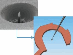
- TEM sample preparation with FIB lift-out solutions for plan-view and backside milling
- Making correlative TEM and atom probe nanowire samples
- Creating high quality samples for improved TEM, EDS and / or EBSD and other types of analysis where either sample thickness or shadowing may otherwise be a problem
- Neutralising highly charging areas on uncoated insulating specimens
- Measurement of electrical parameters of nanostructures
 Benefits Include (depending on model):
- Port-Mounted, Freeing up Stage & Chamber Space
- Move Linearly in ANY direction with nanometre precision
- Ability to change Tips without Venting
- Quickly Reorient Samples In Situ
- Perform Electrical & Nano-mechanical Testing
- Easily Perform Nanomanipulation Tasks using the stage frame of reference
- Perform quick and easy ex-situ grid attach using OmniCut® – also allows easy generation of inverted atom probe / TEM tomography samples
- Digital, closed loop, 360 degree probe tip rotation keeping the tip in view for tip shaping or sample repositioning (see images below)
Contact us for more information to see which Autoprobe tool best suits your applications
GAS INJECTION SYSTEMS
OmniGIS II Gas Injection System
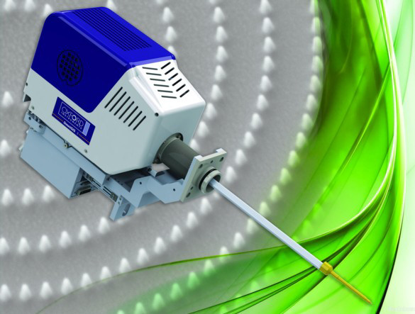
 The OmniGIS II is a revolutionary single port, single nozzle, multiple gas injection system (GIS), enabling users to construct nanostructures in the SEM or FIB with unprecedented precision, speed and usability
Typical applications for the Omniprobe OmniGIS include:
— FAILURE ANALYSIS AND MATERIALS CHARACTERISATION
- Deposit conductive metals for electrical measurements or SPM techniques such as SSRM
- Create nanomarks for sample localisation and TEM lamella end-pointing
- Create strong, reliable Pt welds for nanomanipulation
- Minimise curtaining artefacts in FIB samples by depositing W or C milling masks
- Reduce FIB re-deposition by flowing XeF2 while milling
- Improve imaging and elemental analysis with high contrast, low background protection layers
— GENERATION OF NANOSTRUCTURES
- Make nano-pillars, move nanowires and modify carbon nanotubes
- Customise AFM cantilevers
- Create electron emission tips
- Faster nano-patterns achieved using unique gas flux processes with a wide range of carrier gases
- Create high resolution nanostructures with controlled gas flow to desired target pressures
— DEVELOP NEW PROCESSES
Extend the FIB or SEM to advanced techniques such as atomic layer deposition (ALD) and self-assembled monolayers (SAMS).
- Deliver precursors sequentially in a pre-programmed repetitive sequence to produce ”GIS-ALD” films
- Enable nanoscale imaging, patterning and deposition on commercial SEM or FIB
— NANOLITHOGRAPHY (REQUIRES SCAN GENERATOR)
Perform direct write lithography using an electron or ion beam to accurately pattern nanostructures without the need for a mask.
- Rapid prototyping of bottom-up nano-circuits with single step processes
- No ’proximity effect’ correction required
- Excellent alternative for resist-limited high aspect ratio patterning
- Enable lithography on previously impossible samples
- Immediately characterise results with appropriate accessories
- Enhanced pressure control for optimised lithography
- Contact us for more information


 Benefits Include (depending on model):
 The OmniGIS II is a revolutionary single port, single nozzle, multiple gas injection system (GIS), enabling users to construct nanostructures in the SEM or FIB with unprecedented precision, speed and usability