Enabling results for science and industry
QLD: (07) 4059 0784
VIC: (03) 9681 9192
For sales: sales@nanospec.com.au
For service: service@nanospec.com.au

QLD: (07) 4059 0784
VIC: (03) 9681 9192
For sales: sales@nanospec.com.au
For service: service@nanospec.com.au

EBSD has become a well-established technique for microstructural characterisation in the SEM or FIB. The crystallographic data obtained can be used in the measurement of crystal orientation, misorientation, grain size distribution, texture, strain analysis, recrystallised / deformed fractions and grain boundary characterisation. The technique is used in a broad span of applications in metals & materials analysis / processing, microelectronics and earth sciences.
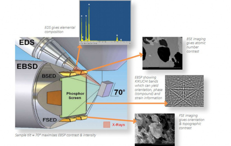
Microstructural EBSD measurements of phase and orientation rely on detecting and analysing electron backscatter (Kikuchi) patterns (or EBSPs) generated in the Scanning Electron Microscope (SEM) from a polycrystalline sample. This information can be acquired simultaneously with EDS data to reveal both sample chemistry and crystal structure on a micro / nano-scale.
Click Here for a brief video demonstration of how EBSD works using Oxford Instruments AZtec HKL.
For more information on EBSD as a technique, visit Oxford Instruments' educational website www.ebsd.com.
Oxford Instruments HKL offer a range of EBSD detectors to suit every application:

AZtec integrates AZtecHKL acquisition and analysis software with the Nordlys EBSD detectors to create a powerful and versatile solution for EBSD.
Contact us for more technical details and application notes.
Visit www.ebsd.com Oxford Instrument’s educational website dedicated to the principles and practice of EBSD